RAM
Random Access Memory (RAM) is a type of computer memory that can be accessed randomly. This means, any random byte can be addressed and accessed without any need to read the preceding bytes.
Physical Properties
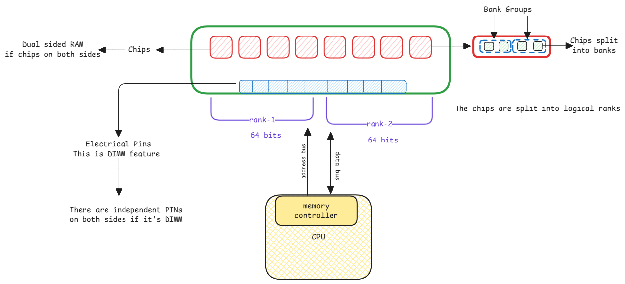
- Channels - It's the number of data paths between the RAM and the CPU. More channels mean more data can be transferred simultaneously. Dual channel means two channels are used but we must use two identical RAM sticks for this to work.
- DIMM - Dual In-line Memory Module is a type of RAM that has pins on both sides of the module. These pins work independently, allowing for more data to be transferred at once.
- Chips - The chips on the RAM module are the actual memory cells that store data. In dual-sided chips, there are chips on both sides of the stick.
- Ranks - It's just a logical division of the memory chips on the RAM module. The memory controller knows which rank to access for a given address. Each Rank is seen by CPU as a different memory module. Each chip is part of only one Rank. This means the available chips are grouped into Ranks.
- Bank - Each chip is then divided into multiple banks. This is a physical division of the memory cells into 2-D arrays inside the chip.
- Bank Group - It's a logical grouping of banks inside a chip but achieved by the physical dedicated circuits that allow simultaneous access to banks in different groups.
The RAM stick itself doesn't contain any firmware. There exists just a serial presence detect (SPD) chip that contains information about the RAM stick, such as its size, ranks, speed, and timings. This information is used by the CPU memory controller.
Interleaving
This is the concept that uses the Ranks and also Bank Groups.
- Request within same ranks but banks of different bank groups can be processed without waiting.
- Request between two different ranks can be processed without waiting.
With dual channel memory, the number of ranks increases. This means, there are 2 memory sticks with 2 ranks each. The 4 ranks and out of which 2 can be accessed at a time.
Address Translation
When the MMU returns the physical address of a location in RAM, the memory controller then converts the physical address into a format that can be used to access the RAM chips.
This means, the generated address will be in the form of a rank, bank, row, and column.
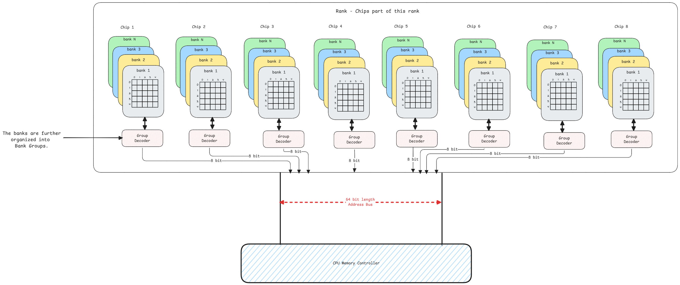
When the address is decoded, all banks in the rank will get the same signal. All banks will have the same row and column selected.
The values from all banks are concatenated to form the full 64 bit data.
Memory Cell
Each memory cell in the RAM is made up of a capacitor and a transistor. The transistor acts as a switch that can either allow or block the flow of current to the capacitor. It's used to read data from the capacitor or to write data to it.
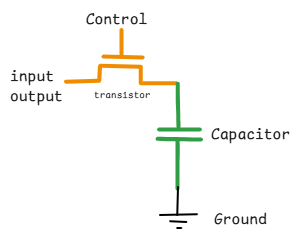
Transistor is a combination of transfer and resistor. Only when the voltage is above a certain threshold, the transistor will allow current to flow through it. This is how it can be used to read or write data.
Word and Bit Line
- Word Line - It's nothing but the row in the RAM chip. When the address is decoded, the word line is activated to select the row. This means the all memory cells in that row is activated for reading or writing.
- Bit Line - It's the column in the RAM chip. Based on the column address, the bit line is selected to read or write data.
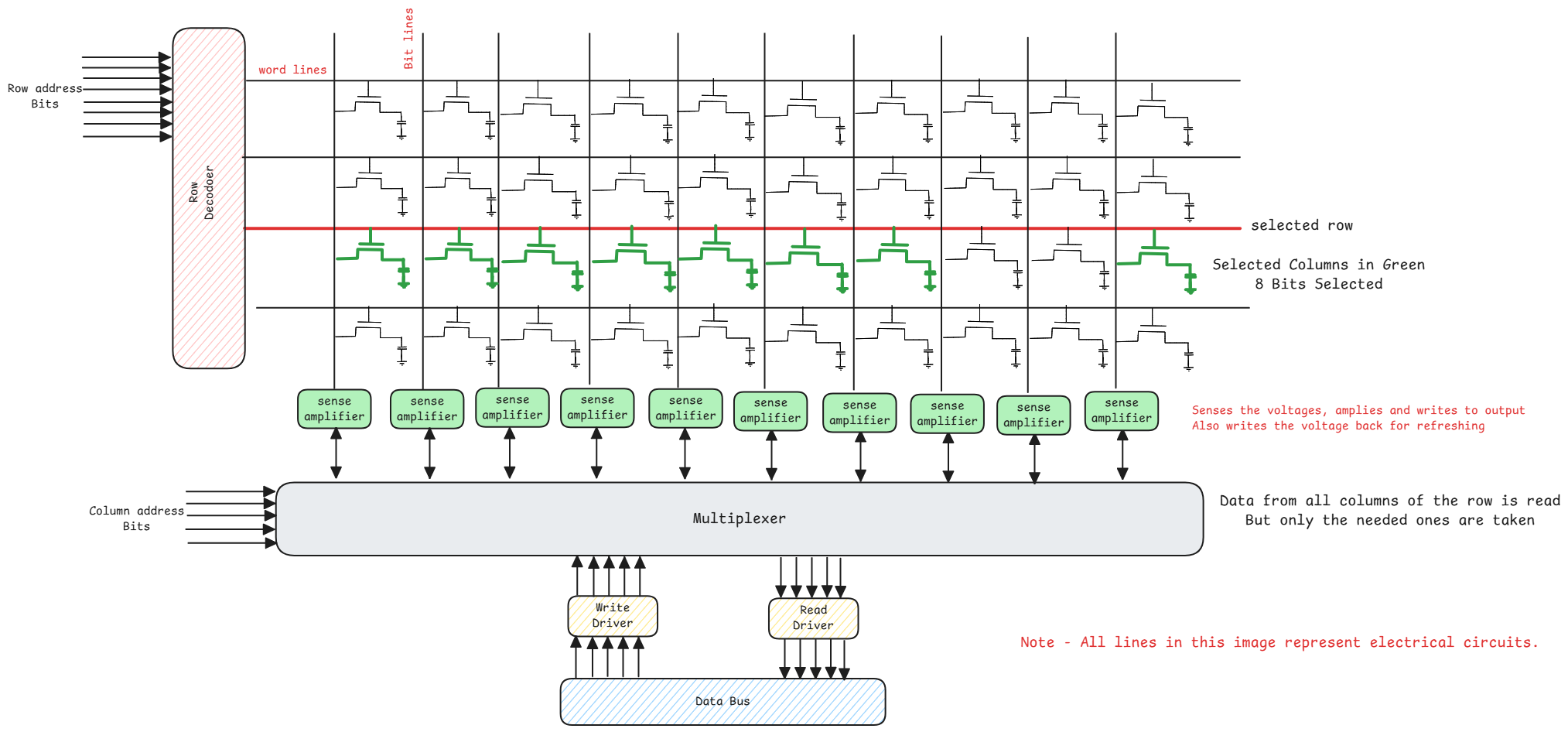
The picture above shows only a small size of the matrix. In reality, the matrix can be huge with many rows and columns.
Bus Size
In most modern systems, the bus size is 64 bits. This means, the data transferred between the RAM and CPU is 64 bits at a time. This is why the RAM chips are designed to have 64 bits of data in each rank.
Still, the CPU cache lines are 64 bytes. The RAM must transfer 8 times the data to fill the cache line. This happens in bursts and multiple CPU cycles.
SRAM vs DRAM
-
SRAM (Static RAM) - This is fast and expensive but needs more space for each bit. It's used in CPU caches. It's called static because it doesn't need to be refreshed like DRAM. The charge written to the cell remains as long as it's needed.
no capacitors neededIn SRAM, each bit is stored in a flip-flop made of transistors, eliminating the need for capacitors. It needs 6 transistors instead.
-
DRAM (Dynamic RAM) - This is slower due to refresh cycles and cheaper since it needs just one transistor and one capacitor for each bit.
It's dynamic because the capacitors lose charge and must be refreshed periodically to maintain the data. DRAM is commonly used for the main memory in computers.
Refresh Cycle
There exist two types of refresh happening in DRAM:
-
Row Refresh - This is when a specific row in the memory is refreshed. The memory controller will read the data from the row and write it back to the same row to restore the charge in the capacitors.
-
Global Refresh - This is when all rows in the memory are refreshed. This is done to ensure that all data is preserved, especially if the memory isn't being accessed frequently.